Where I describe the process of writing and debugging a multitasking program for the Microchip ATtiny13A.
Introduction#
To get the most of any microcontroller, its best to have a framework for multitasking and to ensure it will be as efficient as possible, write it in assembly code. The second aspect to developing the code is debugging it. Which can be problematic, particularly on a chip with limited resources such as the ATtiny13A. This post covers both the code for multitasking and a clever way to determine which tasks are running and for how long.
Overview#
The code for this article and other articles on the ATtiny13A can be found in the ATtiny13A repository. This particular example is examples/asm_oneline.
Multitasking#
This iteration of a multitasking program is a blocking program. Each task will run until complete, then it will give up control to the next task. The tasks are assigned via a table, which allows them to be placed in any order, as many times as desired, however, these decisions need to be made at assembly and not during execution.
Debugging#
I saw an article on a clever mechanism to determine which tasks are running and thought this would be opportunity to write the program and demonstrate the debugging technique. The technique uses the GPIO pins to output a value for each task. The value is converted to a voltage using a simple R-2R ladder digital to analog converter (DAC), which can be viewed via an oscilloscope. This allows you to see which tasks are performed, and the duration of each task.
In the image below, the numbers indicate the task being run, the orange line shows when and how long, each task executed for one cycle through the table.
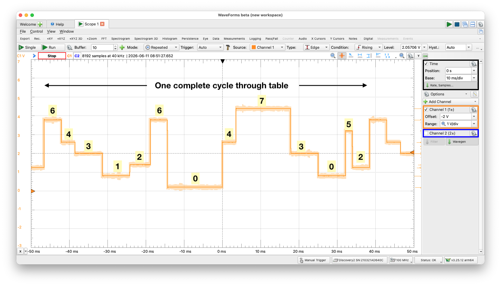
8 tasks, when and duration
Multitasking Program#
Setup#
Setup is typical for most assembly programs, initialize the vectors and registers and set the GPIO pins to be outputs. The last part is critical for it will be the low PORTB pins, PB0-2, which provide the values for the DAC.
Dispatch and Table#
Dispatch is the interesting part, due to the nature of the Z register, the icall instruction and reading program memory. The table contains the addresses of the tasks to be performed. The table entries will be executed in order, starting at the bottom, can be any number of entries (given memory constraints) and a task can be repeated multiple times. The number of entries in the table are automatically computed, NUM_TASKS. A short example of the table is the following:
jump_table:
        .word   pm(task0)
        .word   pm(task5)
        .word   pm(task1)
        .word   pm(task3)
        .word   pm(task7)
...
        .word   pm(task4)
        .word   pm(task6)
jump_table_end:
Dispatch or calling the specific tasks is a little complicated due to the need to use the Z register (r31:r30) for both reading program memory and for calling the task (icall). The steps are:
- Calculate the index
- Get the table address
- Add index and address to find entry address
- Move the address into a temp register
- Load Z with address in temp register
- Execute task call
When the size of the table is reached (via decrement), the process starts over at the bottom of the table.
Tasks#
For this example, the tasks do little, other than assert the value of the task (0-7) and delay for a period of time. I thought it would be valuable to understand the switching costs of each task and the image below shows the 8 tasks, without a delay. The measurement is approximately 24ms, which is 3 clock cycles of a 1.2MHz clock (833.3ns/cycle).
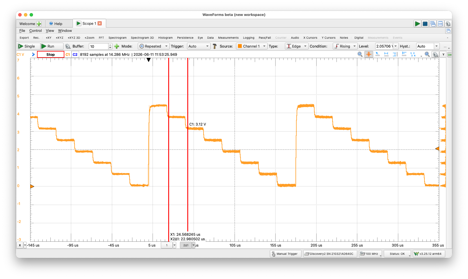
8 tasks with no delay
Debugging#
Idea#
The idea of using the GPIO pins for debugging came from this article in EE Journal. I strongly agree with the author as to Jack Ganssle and the value he brought to embedded software, and thought the idea was brilliant. That said, it didn’t quite work right as portrayed in the article. The article stated the following:
“The following trick will let you monitor as many as eight task IDs with just three of a processor’s GPIO lines and a digital oscilloscope. Instrument the task-switching module by adding code to the module that outputs the task ID number on the three GPIO pins. Then, connect the three GPIO pins to an R-2R ladder DAC, as shown in the graphic below.”
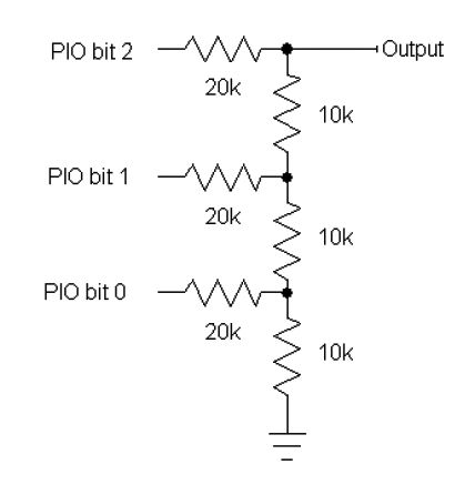
R-2R DAC from article
The issue I had was in modeling the circuit. No matter what I did, the values weren’t symmetrical nor linear. Which in itself, doesn’t mean the idea wasn’t sound. It meant having to know exactly which value went to which task.
Debugging the Idea#
With the help of Claude, I determined that the bottom resistor (R4) needed to be 20K and not 10K. Once I modeled the circuit with these values (see image below), everything made sense. For each increment, the value went up .625V, which meant it was relatively easy to view and understand which task was running. Task 0 would 0V, task 1 would be .625V, task 2, 1.250V and so on.
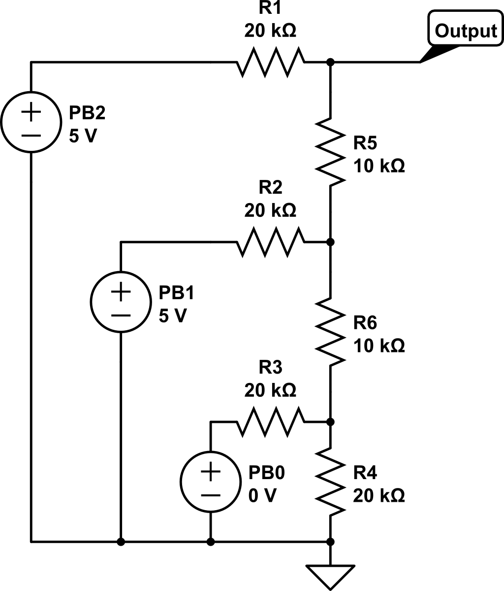
Correct Implementation of R-2R DAC
Having symmetrical and even valued steps for each task made it simple to see when the code wasn’t quite right. While writing this entry, I discovered my dispatch loop wasn’t correct, simply because the image didn’t match the values I expected. Very helpful.
Summary#
I love the idea from Jack Ganssle, and it reminded me of the value he brought to embedded software. I also plan on perusing his site for more ideas which I’ll present here if it makes sense. I also will spend more time, refining this code, and putting it to work. Having a simple multitasking framework, is extremely valuable and opens up more coding ideas for the future!