Where I take the next step in developing PWM code in C for the ATmega328. This time, I create a new analogWrite() in C.
Sources#
- Microchip AVR ATmega328 Go to this page for the datasheet, you will need it.
- Definitive UNO pinout, see below
- avr-libc Standard AVR C Library
- Secrets of Arduino PWM Great tutorial as to how to write code for PWM on the ATmega328
- DIYODE: PWM Classroom Great educational article on PWM and DC Motors
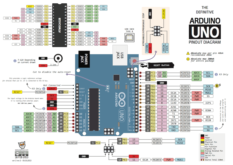
Arduino Uno Pinout
Introduction#
In the previous entry, I demonstrated how you could program the ATmega328 to provide a fast PWM signal on pins 5 and 6. In this entry, I’ll take the example a bit further by adjusting for all 6 pins which can provide a PWM signal. (Those marked by a “~” on the Arduino UNO.) I’ll also continue to refine the table which documents how to program the 6 pins.
While this example will provide another version of analogWrite(), I don’t believe it is superior in coding efficiency. However, it is the one I wrote (and I will explain) so it will be superior as to how to understand it!
The Registers#
It helps to document the registers briefly in the code itself. I created a table which helps me track:
- Columns 1-2: Pin cross reference, Uno to ATmega328
- Columns 3-6: Compare Register tied to pin, Timer/Counter #, Number of bits and Timer/Counter Control Registers
- Column 7: Scalars for clock as they are quite handy for setting frequency and notice they are not the same for the two 8-bit counter/timers!
| Uno | 328 | Reg. | T/C | # | TCCRnn | Scalars |
|---|---|---|---|---|---|---|
| 3 | PD3 | OC2B | 2 | 8 | 2A/2B | 1/8/32/64/256/1024 |
| 5 | PD5 | OC0B | 0 | 8 | 0A/0B | 1/8/64/256/1024 |
| 6 | PD6 | OC0A | 0 | 8 | 0A/0B | 1/8/64/256/1024 |
| 9 | PB1 | OC1A | 1 | 16 | 1A/1B | 1/8/64/256/1024 |
| 10 | PB2 | OC1B | 1 | 16 | 1A/1B | 1/8/64/256/1024 |
| 11 | PB3 | OC2A | 2 | 8 | 2A/2B | 1/8/32/64/256/1024 |
Identifying and Setting the Pins#
As there are only 6 pins used, I use a case statement to match Arduino pin to ATmega328 pin. This allows me to set the specific PWM mode on a per pin basis. I also make some assumptions as to the type of PWM signal. In this case, I only use fast PWM which allows the ATmega328 to provide a fast, non-symmetrical PWM signal. I also follow a similar process as analogWrite() and provide either 488Hz or 976Hz frequencies on the pins. The frequencies are identified up-front and are not adjustable.
I use the same approach I did in the previous PWM entry. For more detail, review, please review that entry.
Using if/else if flow#
In many situations like this, where you are making adjustments to a set of ports, its best to review the code to find duplication then factor out the duplicates. Once this has been done, you can call a function for each of the scenarios.
Note: I took the factoring approach in pinMode() and pinTest(), as for each of the 14 pins the steps are identical. This allowed me to setup a function to perform a step and call it with one of the 14 pins. (see code on GitHub)
In this case, due to each Timer/Counter being a little bit different, there wasn’t value in looking for duplication. In stead, I used a series of if/else if statements to determine which specific pin was being configured and made the specific changes required for the pin. It isn’t an efficient method, however, it seems to be the only way to do it.
You could also look at each instance (pin) and use that instance as an example as to how to configure the pin. For example, in the code:
else if (apin == 9) {
        // set UNO pin 9/PB1, 976.6Hz
you could use the configuration code as an example as to how to configure Timer/Counter 1 for pin 9. I could also review the code and make pin 9, a Phase Correct, PWM Mode signal instead of the mode I used Fast PWM.
The Code: analogWrite()#
/* analogWrite: setup the Timer/Counters to provide a PWM signal
Parameters (Arduino Pin Number, Duty Cycle N (where n/255 = %))

Uno	328	Reg.	T/C	#  TCCRnn	Scalars
3	PD3	OC2B	2	8	2A/2B	1/8/32/64/256/1024
5	PD5	OC0B	0	8	0A/0B	1/8/64/256/1024
6	PD6	OC0A	0	8	0A/0B	1/8/64/256/1024
9	PB1	OC1A	1	16	1A/1B	1/8/64/256/1024
10	PB2	OC1B	1	16	1A/1B	1/8/64/256/1024
11	PB3	OC2A	2	8	2A/2B	1/8/32/64/256/1024

Timer Configurations (n=0,1,2)
TCCRnA - Timer/Counter Control Register A
[ COMnA1 COMnA0 COMnB1 COMnB0 0 0 WGMn1 WGMn0 ]

TCCRnB - Timer/Counter (n=0or2) Control Register B
[ FOCnA FOCnB 0 0 WGM02 CS02 CS01 CS20 ]

TCCR1B - Timer/Counter1 Control Register B
[ ICNC1 ICES1 0 WGM13 WGM12 CS12 CS11 CS10 ]

0. Clear all Timer/Counter Registers
1. Set pin to be output pin
2. Setup Timer Register A
3. Setup Timer Register B
*/

#define delay 500
#include <avr/io.h>
#include <util/delay.h>

void blink (short int times)
{
    // Set the built-in LED PB5 to be an output
    DDRB |= _BV(DDB5);
    // Enter an infinite loop
    for (int i=0;i<times;i++) {
        PORTB |= _BV(PORTB5);
        _delay_ms(delay);
        PORTB &= ~(_BV(PORTB5));
        _delay_ms(delay);
    }
}

void off_led ()
{
    // Set the built-in LED PB5 to be an output
    DDRB |= _BV(DDB5);
    PORTB &= ~(_BV(PORTB5));
}

void clear_all_TC(void) {
    // reset both timer/counter registers
    TCCR0A = 0;
    TCCR0B = 0;
    TCCR1A = 0;
    TCCR1B = 0;
    TCCR2A = 0;
    TCCR2B = 0;
}

short int analogWrite(short int apin, short int cycle) {

    if (apin == 3) {
        // set UNO pin 3/PD3 to output, 488.3Hz
        DDRD |=  _BV(DDD3);

        // TCCR2A [ COM2A1 COM2A0 COM2B1 COM2B0 0 0 WGM21 WGM20 ] = 00100011
        TCCR2A |= (_BV(COM2B1) | _BV(WGM21) | _BV(WGM20));

        // TCCR2B [ FOC2A FOC2B 0 0 WGM22 CS22 CS21 CS20 ]
        TCCR2B |=  (_BV(CS22) | _BV(CS20));

        OCR2B = cycle;
        return(0);
    }
    else if (apin == 5) {
        // set UNO pin 5/PD5 to output, 976.6Hz
        DDRD |=  _BV(DDD5);

        // TCCR0A [ COM0A1 COM0A0 COM0B1 COM0B0 0 0 WGM21 WGM20 ] = 00100011
        TCCR0A |= (_BV(COM0B1) | _BV(WGM21) | _BV(WGM20));

        // TCCR0B [ FOC2A FOC2B 0 0 WGM22 CS22 CS21 CS20 ]
        TCCR0B |=  (_BV(CS21) | _BV(CS20));

        OCR0B = cycle;
        return(0);
    }
    else if (apin == 6) {
        // set UNO pin 6/PD6 to output, 976.6Hz
        DDRD |=  _BV(DDD6);

        // TCCR0A [ COM0A1 COM0A0 COM0B1 COM0B0 0 0 WGM21 WGM20 ] = 11000010
        TCCR0A |= (_BV(COM0A1) | _BV(COM0A0) | _BV(WGM21) | _BV(WGM20));

        // TCCR0B [ FOC2A FOC2B 0 0 WGM22 CS22 CS21 CS20 ]
        TCCR0B |=  (_BV(CS21) | _BV(CS20));

        OCR0A = cycle;
        return(0);
    }
    else if (apin == 9) {
        // set UNO pin 9/PB1, 976.6Hz
        DDRB |=  _BV(DDB1);

        // TCCR1A [ COM1A1 COM1A0 COM1B1 COM1B0 0 0 WGM11 WGM10 ] = 10000001
        TCCR1A |= (_BV(COM1A1) | _BV(WGM10));

        // TCCR1B [ 1CNC1 1CES1 0 WGM13 WGM12 CS12 CS11 CS10 ]
        TCCR1B |= (_BV(WGM12) | _BV(CS11) | _BV(CS10));

        OCR1A = cycle;
        return(0);
    }
    else if (apin == 10) {
        // set UNO pin 10/PB2 to output, 976.6Hz
        DDRB |=  _BV(DDB2);

        // TCCR1A [ COM1A1 COM1A0 COM1B1 COM1B0 0 0 WGM11 WGM10  ] = 00100001
        TCCR1A |= (_BV(COM1B1) | _BV(WGM10));

        // TCCR1B [ 1CNC1 1CES1 0 WGM13 WGM12 CS12 CS11 CS10 ]
        TCCR1B |= (_BV(WGM12) | _BV(CS11) | _BV(CS10));

        OCR1B = cycle;
        return(0);
    }
    else if (apin == 11) {
        // set UNO pin 11/PB3 to output, 488.3Hz
        DDRB |=  _BV(DDB3);

        // TCCR2A [ COM2A1 COM2A0 COM2B1 COM2B0 0 0 WGM21 WGM20 ] = 10000011
        TCCR2A |= (_BV(COM2A1) | _BV(WGM21) | _BV(WGM20));

        // TCCR2B [ FOC2A FOC2B 0 0 WGM22 CS22 CS21 CS20 ]
        TCCR2B |= (_BV(CS22) | _BV(CS20));

        OCR2A = cycle;
        return(0);
    }
    else {
        return(1);
    }
}

int main (void)
{
    clear_all_TC();

    short int ard, duty_cycle;

    ard = 11;
    duty_cycle = 63; // 63 = 25%
    if (analogWrite(ard, duty_cycle)) {
        blink(5);
    }

    ard = 10;
    duty_cycle = 32;
    if (analogWrite(ard, duty_cycle)) {
        blink(6);
    }
    off_led();
}
Comments on PWM#
- If WGM = 7, then COM0A1:0 must be set to 1 for OC0A to to toggle (see page 109). In other words, setting WGM to 7, changes the TOP from xFF to the contents of OC0A. Which will change the frequency on OC0B. If this sounds confusing, it is. I would avoid WGM = 7 (and use WGM = 3). I was able to create this waveform on T/C0 with WGM = 7. The specific code is posted below as well.
- CH1 is Pin 6, at 976Hz, 50% duty cycle
- CH2 is Pin 5, at 1.94kHz, 50% duty cycle
I wasn’t able to create a waveform consistently based on what I thought, so I’m not going to attempt to explain more.
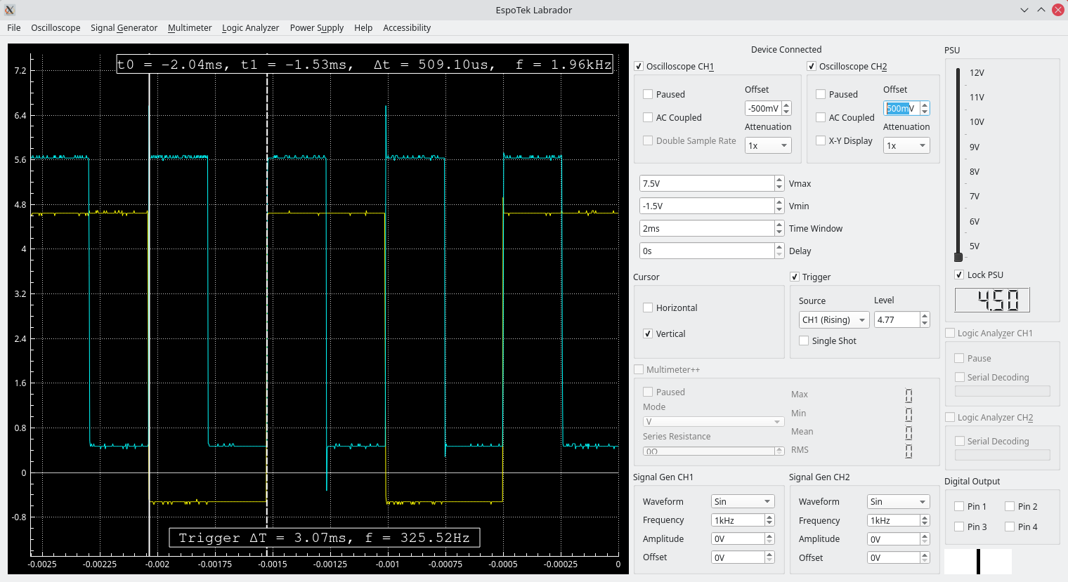
Fast PWM with WGM=7 on T/C 0
    else if (apin == 5) {
        // set UNO pin 5/PD5 to output, 976.6Hz
        DDRD |=  _BV(DDD5);

        // TCCR0A [ COM0A1 COM0A0 COM0B1 COM0B0 0 0 WGM21 WGM20 ] = 00100011
        TCCR0A |= (_BV(COM0B1) | _BV(WGM21) | _BV(WGM20));

        // TCCR0B [ FOC2A FOC2B 0 0 WGM22 CS22 CS21 CS20 ]
        TCCR0B |=  (_BV(WGM22) | _BV(CS21) | _BV(CS20));

        OCR0B = cycle;
        return(0);
    }
    else if (apin == 6) {
        // set UNO pin 6/PD6 to output, 976.6Hz
        DDRD |=  _BV(DDD6);

        // TCCR0A [ COM0A1 COM0A0 COM0B1 COM0B0 0 0 WGM21 WGM20 ] = 11000010
        TCCR0A |= (_BV(COM0A0) | _BV(WGM21) | _BV(WGM20));

        // TCCR0B [ FOC2A FOC2B 0 0 WGM22 CS22 CS21 CS20 ]
        TCCR0B |=  (_BV(CS21) | _BV(CS20));

        OCR0A = cycle;
        return(0);
    }
...
    ard = 6;
    duty_cycle = 127; // 127 = 50%
    if (analogWrite(ard, duty_cycle)) {
        blink(2);
    }

    ard = 5;
    duty_cycle = 63; // 63 = 25%
    if (analogWrite(ard, duty_cycle)) {
        blink(4);
    }